Purpose
The RT9465 is a switch-mode single cell li-Ion/Li-Polymer battery charger for portable applications. It intergrates a synchronous PWM controller, and high accuracy voltage regulation. Besides, the charging current is regulated through the integrated sensing resistors. This document explains the function and use of the RT9465 evaluation board (EVB), and provides information to enable operation, modification of the evaluation board and circuit to suit individual requirements.
Introduction
General Product Information
The RT9465 is a switch-mode single cell li-Ion/Li-Polymer battery charger for portable applications. It integrates a synchronous PWM controller, and high accuracy voltage regulation. Besides, the charging current is regulated through the integrated sensing resistors.
Product Feature
- Input Voltage Range : 3.9V to 14V
- Synchronous 1.5MHz/0.75MHz Switching Frequency 95% Max. Duty
- Up to 92%/94% Peak Efficiency at VIN = 9V/5V
- VIN Over-Voltage Protection : 14.5V
- VIN Under-Voltage Protection : 3.8V
- VIN Under-Voltage-Lock-Out : 3.3V
- Fault Detection (VIN and VBAT Monitoring)
- INT Output for Communication with I2C
- Programmable Minimum Input Voltage Range : 3.9V to 13.4V (0.1V/Step)
- Programmable Battery Voltage Regulation Range : 3.8V to 5.06V (0.02V/Step)
- Programmable End of Charge Range : 0.6A to 1.6A (0.1A/Step)
- Programmable Average Output Current Regulation Range : 0.6A to 3A (0.1A/Step)
- Junction Temperature Monitor : 60°C to 116°C (4°C/Step)
- VIN Minimum Input Voltage Regulation (MIVR) : ±3%
- Battery CV (Constant Voltage) Regulation : ±1%
- Output CC (Constant Current) Regulation, Output Current < 1A : ±100mA (VBUS = 9V/12V)
- Output CC (Constant Current) Regulation, Output Current > 1A : ±10% (VBUS = 9V/12V)
- Junction Temperature Monitor : ±3°C
- Thermal Shutdown : 160°C
Key Performance Summary Table
|
Key Features
|
Evaluation Board Number : PCB096_V1
|
|
Input Voltage
|
3.9V to 14V
|
|
Output Voltage
|
3.8V to 5.06V
|
|
Max Output Current
|
3A
|
|
Package Type
|
RT9465GQW, WQFN-16L 3x3 (W-Type)
|
Bench Test Setup Conditions
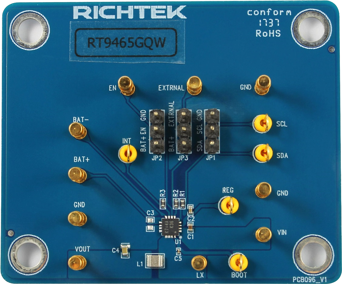
Headers Description and Placement
Carefully inspect all the components used in the EVB according to the following Bill of Materials table, and then make sure all the components are undamaged and correctly installed. If there is any missing or damaged component, which may occur during transportation, please contact our distributors or e-mail us at evb_service@richtek.com.
Test Points
The EVB is provided with the test points and pin names listed in the table below.
|
Test point/
Pin name
|
Signal
|
Comment (expected waveforms or voltage levels on test points)
|
|
VIN
|
Input Voltage
|
DC input power supply
|
|
VOUT
|
Output Voltage
|
Battery connection point to positive terminal of the battery pack.
|
|
GND
|
Ground
|
Ground.
|
|
BAT+
|
Positive Battery Voltage Sense
|
Positive battery voltage sense. Conect to battery connector.
|
|
BAT-
|
Negative Battery Voltage Sense
|
Negative battery voltage sense. Conect to battery connector.
|
|
EN
|
Enable Pin
|
Device enable control pin. Pull low to disable device. I2C not available
when disabled.
|
|
INT
|
Intterrupt
|
Open drain interrupt output. connect to pull-up voltage via 10kΩ pull-up resistor. Normally high, the INT pin sends an active low.
|
|
SDA
|
SDA
|
I2C interface data. Connect to pull-up voltage via 10kΩ pull-up resistor.
|
|
SCL
|
SCL
|
I2C interface clock. Connect to pull-up voltage via 10kΩ pull-up resistor.
|
|
LX
|
Switch node
|
Switch node. Connect to an external inductor
|
|
EXTRNAL
|
External Pull Up Voltage
|
External pull up voltage. Connect to power supply
|
|
REG
|
REG
|
PWM low-side driver and bootstrap power supply.
|
|
BOOT
|
BOOT
|
Bootstrap supply for high-side MOSFET. Connect a capacitor between BOOT and LX.
|
Power-up & Measurement Procedure
1. Connect input power (5V < VBUS < 14V) and input ground to VIN and GND test pins respectively.
2. Connect positive end and negative terminals of VBAT to VOUT and GND test pins respectively.
3. There is a 3-pin header (JP3) for pull-up control. To use a jumper at “EXTRNAL” option to tie pull up pin to external pull up voltage. Use a jumper at “BAT+” option to tie pull-up test pin to battery.
4. Connect EN pin to 3.3V to enable device and use I2C to enable charger.
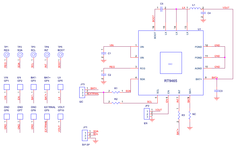
Schematic, Bill of Materials & Board Layout
EVB Schematic Diagram
Bill of Materials
|
Reference
|
Qty
|
Part Number
|
Description
|
Package
|
Manufacturer
|
|
U1
|
1
|
RT9465GQW
|
Switching Charger
|
WQFN-16L 3x3
|
RICHTEK
|
|
C1
|
1
|
GRM155R61E225KE11
|
2.2µF/25V/X5R
|
C-0402
|
muRata
|
|
C2
|
1
|
GRM155R60J475ME47
|
4.7µF/6.3V/X5R
|
C-0402
|
muRata
|
|
C4
|
1
|
GRM188R61A106KE69
|
10µF/10V/X5R
|
C-0603
|
muRata
|
|
C5
|
1
|
GRM033R61C473KE84
|
47nF/16V/X5R
|
C-0201
|
muRata
|
|
L1
|
1
|
DFE252012F-1R0M
|
1µH
|
2.5x2.0x1.2mm
|
muRata
|
|
R1, R2, R3
|
3
|
NCP15XH103F03RC
|
10k
|
R-0402
|
muRata
|
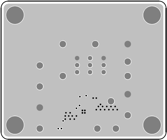
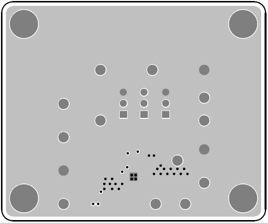
PCB Layout
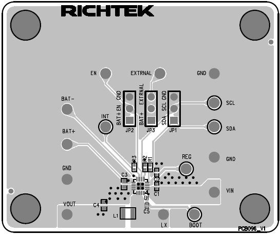
Top View (1st layer)
PCB Layout—Inner Side (2nd Layer)
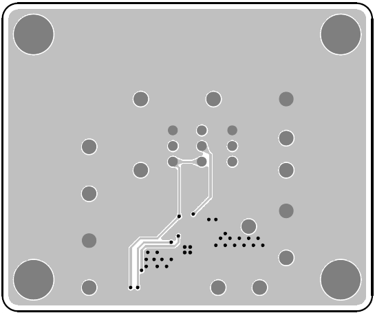
PCB Layout—Inner Side (3rd Layer)
Bottom View (4th Layer)